Title: A Novel Approach to Design Obfuscated Circuits for Digital Signal Processing Applications Using High-Level Transformations
Authors: Poornima Vemula, Shaik Mohammed Rafi & Raju Katru
Organisation: Malla Reddy Engineering College for Women
Abstract— The goal is to design DSP circuits that are harder to reverse engineer. High-level transformations of iterative data-flow graphs have been exploited for area-speed-power tradeoffs. This is the first attempt to develop a design flow to apply high-level transformations that not only meet these tradeoffs but also simultaneously obfuscate the architectures both structurally and functionally. Several modes of operations are introduced for obfuscation where the outputs are meaningful from a signal processing point of view, but are functionally incorrect. Examples of such modes include a third-order digital filter that can also implement a sixth-order or ninth-order filter in a time-multiplexed manner. The latter two modes are meaningful but represent functionally incorrect modes. Multiple meaningful modes can be exploited to reconfigure the filter order for different applications. Other modes may correspond to no meaningful modes. A correct key input to an FSM activates a reconfiguration. The configure data controls various modes of the circuit operation. Functional obfuscation is accomplished by requiring use of the correct initialization key, and configure data. Wrong initialization key fails to enable the reconfiguration, and a wrong configure data activates either a meaningful but nonfunctional or non-meaningful mode. Probability of activating the correct mode is significantly reduced leading to an obfuscated DSP circuit. Structural obfuscation is also achieved by the proposed methodology via high-level transformations. Experimental results show that the overhead of the proposed methodology is small, while a strong obfuscation is attained. For example, the area overhead for a (3l)th-order IIR filter benchmark is only 17.7% with a 128-bit configuration key, where 1 ≤ l ≤ 8, i.e., the order of this filter should be a multiple of 3, and can vary from 3 to 24.
Index Terms— Digital signal processing (DSP), functional obfuscation, hardware security, high-level transformations, intellectual property (IP) protection, obfuscation, reconfigurable design, structural obfuscation.
INTRODUCTION
Digital signal processing (DSP) plays a critical role in numerous applications, such as video compression, portable systems/computers, multimedia, wired and wireless communications, speech processing, and biomedical signal processing. However, as electronic devices become increasingly interconnected and pervasive in people’s lives, security, trustworthy computing, and privacy protection have emerged as important challenges for the next decade. It is estimated that as much as 10% of all high-tech products sold globally are counterfeit which leads to a conservative estimate of $100 billion of revenue loss [1]. Therefore, DSP system designers have to pay more attention to the security perspective of DSP circuits, since the adversary can easily learn the functionality using massive attacking methods. The problem of hardware security is a serious concern that has led to a lot of work on hardware prevention of piracy and intellectual property (IP), which can be broadly classified into two main categories: 1) authentication-based approach and 2) obfuscation-based approach. The authentication based approaches include physical un-clonable functions (PUFs)-based authentication [2], digital watermarking [3]–[6], key-locking scheme [7], [8], and hardware metering [9]. The focus of this paper is on obfuscation, which is a technique that transforms an application or a design into one that is functionally equivalent to the original but is significantly more difficult to reverse engineer. Some hardware protection methods are achieved by altering the human readability of the hardware description language (HDL) code, or by encrypting the source code based on cryptographic techniques [10]. Recently, a number of hardware obfuscation schemes have been proposed that modify the finite-state machine (FSM) representations to obfuscate the circuits [11]–[13]. However, to the best of our knowledge, no obfuscation based IP protection approach has been proposed specifically for DSP circuits in the literature. This paper, for the first time, presents design of obfuscated DSP circuits via high-level transformations that are harder to reverse engineer. From this standpoint of view, a DSP circuit is more secure, if it is harder for the adversary to discover its functionality even if the adversary can physically tamper the device. In other words, a high level of security is achieved if the functionality of a DSP circuit is designed to be hidden from the adversary. The key contribution of this paper is a novel approach to design obfuscated DSP circuits by high-level transformations during the design stage. The DSP circuits are obfuscated by introducing an FSM whose state is controlled by a key. The FSM enables a reconfiguration that configures the functionality mode of the DSP circuit. High-level transformations lead to many equivalent circuits and all these create ambiguity in the structural level. High-level transformations also allow design of circuits using same data path but different control circuits. Different variation modes can be inserted into the DSP circuits for obfuscation. While some modes generate outputs that are functionally incorrect, these may represent correct outputs under different situations, since the output is meaningful from a signal processing point of view. Other modes would lead to no meaningful outputs. The initialization key and the configure data must be known for the circuit to work properly. Consequently, the proposed design methodology leads to a DSP circuit that is both structurally and functionally obfuscated.
EXISTING OBFUSCATION METHODS
As this paper is the first attempt to develop a methodology to obfuscate DSP circuits by utilizing high-level transformations, it is hard to compare with other existing obfuscation methods which are general to a wide variety of designs. Therefore, we have introduced two metrics to analyze the security, Most of the hardware obfuscation techniques in this paper can also be applied to DSP circuits. However, the use of high-level transformations from a security perspective has not been incorporated into any of these prior hardware obfuscation techniques. In addition, other circuit locking techniques only achieve protection at one-level (i.e., encrypt the normal functionality by a key), while our proposed methodology provides a two-level protection (i.e., structural obfuscation and functional obfuscation). The main advantage of the proposed methodology is the generation of meaningful variation modes from a signal processing point of view, since the meaningful modes create ambiguity to the adversary such that it is hard for the adversary to distinguish the desired functionality from other variation modes. Other existing methods, such as [6], [7], are not specific to DSP circuits, which would not be able to ensure meaningful variation modes from a signal processing point of view. In addition, meaningful variation modes enable our proposed design methodology to be adaptable to reconfigurable applications. Finally, when considering the metrics of the design performance, our proposed methodology is also superior. While our proposed approach only alters the logic of switches, most of the existing methods are based on explicit FSM modifications (e.g., the technique proposed in [13]), which are not scalable since the construction of the FSM is not practical for even moderate-sized circuits, not to mention that the number of added obfuscation states can be relatively large as compared with the original FSM. In our proposed methodology, area consumption is slightly increased due to the increased cost of the control logic for the obfuscated switches.
OBFUSCATED DESIGN VIA HIGH-LEVEL TRANSFORMATIONS
A. Secure Switch Design:-
It can be seen that the DSP circuits can be obfuscated via high-level transformations by appropriately designing the switches in a secure manner. The switches generated by high-level transformations are periodic N-to-1 switches. These switches can be implemented as multiplexers, whose control signals are obtained from ring counters (as shown in Fig. 1).
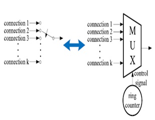
Fig. 1. Switch implementation
Thus, the security of the switch relies upon design of the ring counters such that the outputs of the ring counters can be obfuscated. A ring counter is often modeled as an FSM. An FSM is usually defined by a 6-tuple (I, O, S, S0, F, G), where S is a finite set of internal states, I and O represent the inputs and outputs of the FSM, respectively, F is the next-state function, G is the output function, and S0 is the initial state. However, unlike general FSMs, the FSM of a ring counter is input independent, such that it always transits to the next state based on the current state. As a result, the control signal of the switches (i.e., output of the FSM) will be periodic.
B. Reconfigurable Switch :-
Design Indeed, existing works have demonstrated that functional obfuscation can be achieved by embedding a well-hidden FSM (i.e., obfuscating FSM) in the circuit to control the functionality based on a key [12], [13], [29]. In order to achieve design obfuscation by using high-level transformations, we propose a reconfigurable switch design. The detailed implementation is shown in Fig. 2,
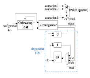
Fig.2. Complete reconfigurable switch design.
where SR represents the state registers that store the information of the current state. We employ the idea of hardware design obfuscation as an activation sequence required before configuration by inserting an obfuscating FSM. The FSM enables a reconfigurator that controls the functionality mode of the DSP circuit by configuring the output function G, next-state function F, and the initial state S0. In our design, the configuration key must be known for the circuit to work properly, which consists of two parts: an L-bit initialization key and a K-bit configure data, as shown in Fig. 10. The initialization key is used as the input of the obfuscating FSM, while the configure data are applied to the reconfigurator to control the operation of the switches. As the configuration of the switch is only enabled after receiving a correct initialization key, hostile attempts of the configure data cannot be processed by the reconfigurator as the reconfigurator is not activated. Note that other secure switch designs, whose detailed switch instances are hidden to the adversary, can also be adopted in the framework. The number of possible variations of ring counters is limited by the length of the configure data, K. We can create M variation modes of the original circuits that have different functionalities, while log2M should be less than or equal to the length of configure data, K. Different configure data can be mapped into the same mode. An example of the mapping between the configure data and the associated modes is illustrated in Table I. Note that this only involves simple combinational logic synthesis.
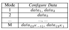
TABLE I:- SWITCH CONFIGURATIONS
DESIGN FLOW OF THE PROPOSED DSP CIRCUIT OBFUSCATION APPROACH
A. Design Methodology
In this section, we propose a novel DSP hardware protection methodology through obfuscation by hiding functionality via high-level transformations. This approach helps the designer to protect the DSP design against piracy. The detailed design flow is described below
Step 1: DSP Algorithm: This step generates the DSP algorithm based on the DSP application.
Step 2: High-Level Transformation Selection: Based on the specific application, appropriate high-level transformation should be chosen according to the performance requirement (e.g., area, speed, power, or energy).
Step 3: Obfuscation via High-Level Transformation: Selected high-level transformations are applied simultaneously with obfuscation where variation modes, and different configurations of the switch instances are designed.
Step 4: Secure Switch Design: The secure switch is designed based on the variations of high-level transformations. Note that different configure data could be mapped into the same mode, which only involves simple combinational logic synthesis.
Step 5: Two-Level FSM Generation: The reconfigurator and the obfuscating FSM are incorporated into the DSP design as shown in Fig. 1. The configuration key is generated at this step.
Step 6: Design Specification: This step includes the HDL and netlist generation and synthesis of the DSP system. After these design steps, designer sends the obfuscated design to the foundry that manufactures the DSP circuit. By using the proposed design methodology, the manufacturer will not gain access to the desired functionality or the configuration key. Unauthorized copies of the obfuscated DSP circuits would provide little information to the adversary. The relationship between the obfuscated design and the original design via high-level transformation is shown in Fig. 3. The only difference between the obfuscated design and the original design via high-level transformation is the control of the DSP circuit.
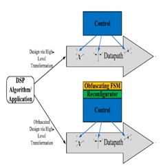
Fig. 3. Relationship between the obfuscated design and the original design
The main datapath is unaltered. As a result, the critical path would not increase for the obfuscated design. Furthermore, the proposed design methodology does not require significant changes to established verification and testing flows. In fact, the obfuscated DSP circuit with the correct key behaves just like the original circuit.
B. Architecture of the Obfuscated:-
DSP Circuits The complete system of the proposed obfuscated DSP circuit is shown in Fig. 4. The reconfigurator will be enabled only by the correct initialization key. Only the correct con- figure data leads to the desired design. A wrong configure data activates an obfuscated mode (either a meaningful or nonmeaningful).
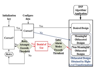
Fig. 4 Architecture of the proposed obfuscated DSP circuit.
The obfuscating FSM and a portion of nonmeaningful variation modes (i.e., we denote as alarm modes) can both be utilized for security check purpose. For example, some undesired modes in Table I can be designed as alarm modes by adding another output signal to the combinational logic. We can improve the security by mapping a larger number of configure data to this alarm mode, while keeping the portion of functional configure data to be relatively small. If the circuit continuously receives wrong initialization key or configure data whose number exceeds the predefined threshold, the adversary is prevented from further attempts of the configuration key by a denial of use block.
CONCLUSION
This paper presents a novel low-overhead solution to design DSP circuits that are obfuscated both structurally and functionally by utilizing high-level transformation techniques. It is shown that verifying the equivalence of DSP circuits by employing high-level transformations will be harder if some switches can be designed in such a way that are difficult to trace. A secure reconfigurable switch design is incorporated into the proposed design scheme to improve the security. A complete design flow is presented. In the proposed obfuscation methodology, the variation modes and the additional obfuscating circuits could also be designed systematically based on the high-level transformations. Compared with other existing obfuscation methods, another advantage of the proposed methodology is the generation of meaningful variation modes from a signal processing point of view, since the meaningful modes create ambiguity to the adversary such that it is hard for the adversary to distinguish the correct functionality from other variation modes. Experimental results have demonstrated the effectiveness of the proposed methodology. This paper, for the first time, considers the security perspective of high-level transformations. Future work will explore the algorithmic aspect of different high-level transformations for design obfuscation. Ongoing work includes the validation of the security performances of meaningful modes and non-meaningful modes. We are also interested in addressing the attack methods of DSP circuits. We intend to exploit the security perspective of the proposed methodology by performing various attacks to the obfuscated DSP circuits. Future work will be directed toward developing a complete design flow which can generate the target structure and obfuscation variation modes automatically based on the specific application performance requirement. The ultimate goal is to develop an electronic design automation synthesis tool which can incorporate large number of design obfuscation algorithms based on high-level transformations for DSP system design.
FURTHERMORE
The approach presented in this paper will prevent piracy from overproduction and mask theft, because the manufacturer would not have access to either the initialization key or the configure data. These keys could be programmed by another honest vendor after the chips have been fabricated or provided to the customers by the designer. Therefore, overproduced chips without the correct keys cannot function properly.
REFERENCES
[1] J. Guajardo, S. S. Kumar, G.-J. Schrijen, and P. Tuyls, “Brand and IP protection with physical unclonable functions,” in Proc. IEEE Int. Symp. Circuits Syst., May 2008, pp. 3186–3189.
[2] G. E. Suh and S. Devadas, “Physical unclonable functions for device authentication and secret key generation,” in Proc. 44th Annu. Design Autom. Conf., Jun. 2007, pp. 9–14.
[3] A. L. Oliveira, “Techniques for the creation of digital watermarks in sequential circuit designs,” IEEE Trans. Comput.-Aided Design Integr. Circuits Syst., vol. 20, no. 9, pp. 1101–1117, Sep. 2001.
[4] D. Kirovski, Y.-Y. Hwang, M. Potkonjak, and J. Cong, “Intellectual property protection by watermarking combinational logic synthesis solutions,” in Proc. Int. Conf. Comput.-Aided Design, Nov. 1998, pp. 194–198.
[5] A. B. Kahng et al., “Watermarking techniques for intellectual property protection,” in Proc. 35th Annu. Design Autom. Conf., Jun. 1998, pp. 776–781.
[6] F. Koushanfar and Y. Alkabani, “Provably secure obfuscation of diverse watermarks for sequential circuits,” in Proc. Int. Symp. Hardw.-Oriented Security Trust, Jun. 2010, pp. 42–47.
[7] J. A. Roy, F. Koushanfar, and I. L. Markov, “EPIC: Ending piracy of integrated circuits,” in Proc. Conf. Design, Autom. Test Eur., Mar. 2008, pp. 1069–1074.
[8] W. P. Griffin, A. Raghunathan, and K. Roy, “CLIP: Circuit level IC protection through direct injection of process variations,” IEEE Trans. Very Large Scale Integr. (VLSI) Syst., vol. 20, no. 5, pp. 791–803, May 2012.
[9] Y. M. Alkabani and F. Koushanfar, “Active hardware metering for intellectual property protection and security,” in Proc. USENIX Security Symp., Aug. 2007, pp. 291–306.
[10] T. Batra. (2005). Methodology for Protection and Licensing of HDL IP [Online]. Available: http://www.design-reuse.com/articles/12745
[11] R. S. Chakraborty and S. Bhunia, “Hardware protection and authentication through netlist level obfuscation,” in Proc. Int. Conf. Comput.-Aided Design, Nov. 2008, pp. 674–677.
[12] R. S. Chakraborty and S. Bhunia, “RTL hardware IP protection using key-based control and data flow obfuscation,” in Proc. 23rd Int. Conf. VLSI Design, Jan. 2010, pp. 405–410.
[13] R. S. Chakraborty and S. Bhunia, “HARPOON: An obfuscationbased SoC design methodology for hardware protection,” IEEE Trans. Comput.-Aided Design Integr. Circuits Syst., vol. 28, no. 10, pp. 1493–1502, Oct. 2009. [14] Y. Lao and K. K. Parhi, “Protecting DSP circuits through obfuscation,” in Proc. IEEE Int. Symp. Circuits Syst., Jun. 2014.
[15] K. K. Parhi, “Algorithm transformation techniques for concurrent processors,” Proc. IEEE, vol. 77, no. 12, pp. 1879–1895, Dec. 1989.
[16] K. K. Parhi and D. G. Messerschmitt, “Pipeline interleaving and parallelism in recursive digital filters. I. Pipelining using scattered look-ahead and decomposition,” IEEE Trans. Acoust., Speech, Signal Process., vol. 37, no. 7, pp. 1099–1117, Jul. 1989.
[17] K. K. Parhi, C. Y. Wang, and A. P. Brown, “Synthesis of control circuits in folded pipelined DSP architectures,” IEEE J. Solid-State Circuits, vol. 27, no. 1, pp. 29–43, Jan. 1992.
[18] K. K. Parhi and D. G. Messerschmitt, “Static rate-optimal scheduling of iterative data-flow programs via optimum unfolding,” IEEE Trans. Comput., vol. 40, no. 2, pp. 178–195, Feb. 1991.
[19] K. K. Parhi, “Pipelining in algorithms with quantizer loops,” IEEE Trans. Circuits Syst., vol. 38, no. 7, pp. 745–754, Jul. 1991.
[20] K. K. Parhi, “Low-energy CSMT carry generators and binary adders,” IEEE Trans. Very Large Scale Integr. (VLSI) Syst., vol. 7, no. 4, pp. 450–462, Dec. 1999.
[21] K. K. Parhi, “Design of multigigabit multiplexer-loop-based decision feedback equalizers,” IEEE Trans. Very Large Scale Integr. (VLSI) Syst., vol. 13, no. 4, pp. 489–493, Apr. 2005.
[22] N. R. Shanbhag and K. K. Parhi, “Relaxed look-ahead pipelined LMS adaptive filters and their application to ADPCM coder,” IEEE Trans. Circuits Syst. II, Analog Digit. Signal Process., vol. 40, no. 12, pp. 753–766, Dec. 1993.
[23] J. Ma, K. K. Parhi, and E. F. Deprettere, “Annihilation-reordering look-ahead pipelined CORDIC-based RLS adaptive filters and their application to adaptive beamforming,” IEEE Trans. Signal Process., vol. 48, no. 8, pp. 2414–2431, Aug. 2000.
[24] C.-Y. Wang and K. K. Parhi, “High-level DSP synthesis using concurrent transformations, scheduling, and allocation,” IEEE Trans. Comput.- Aided Design Integr. Circuits Syst., vol. 14, no. 3, pp. 274–295, Mar. 1995.
[25] K. K. Parhi, VLSI Digital Signal Processing Systems: Design and Implementation. New York, NY, USA: Wiley, 1999.
[26] K. K. Parhi, “Hierarchical folding and synthesis of iterative data flow graphs,” IEEE Trans. Circuits Syst. II, Exp. Briefs, vol. 60, no. 9, pp. 597–601, Sep. 2013.
[27] K. K. Parhi, “Verifying equivalence of digital signal processing circuits,” in Proc. 46th Asilomar Conf. Signals, Syst. Comput., Nov. 2012, pp. 99–103.
[28] K. K. Parhi, “A systematic approach for design of digit-serial signal processing architectures,” IEEE Trans. Circuits Syst., vol. 38, no. 4, pp. 358–375, Apr. 1991.
[29] Y. Alkabani, F. Koushanfar, and M. Potkonjak, “Remote activation of ICs for piracy prevention and digital right management,” in Proc. Int. Conf. Comput.-Aided Design, Nov. 2007, pp. 674–677
To download the above paper in PDF format Click on below Link: